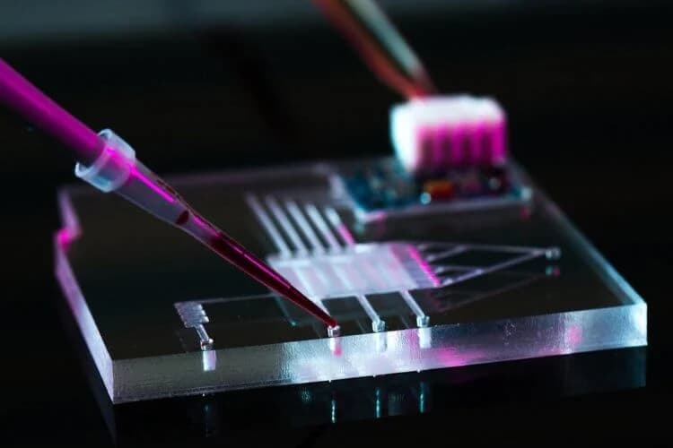
Nanocrystal electricity is an emerging technology that utilizes the unique properties of nanocrystals to improve electrical conductivity and efficiency. Nanocrystals are tiny crystals on the nanometer scale, generally ranging from 1 to 100 nanometers in size. At this incredibly small size, nanocrystals exhibit quantum mechanical properties that affect their electrical behaviors in ways not seen in larger materials. The tunable nature of nanocrystals allows researchers to engineer their band gap structure to achieve desired electrical characteristics. When incorporated into devices and materials, these nanocrystal properties can allow electrons to flow more smoothly, lowering resistance and power loss. Nanocrystal electricity has the potential to revolutionize many areas of electronics and energy technology, enabling significant advances in how we generate, store, transmit, and use electrical power. However, the technology is still in its early stages, with challenges to overcome before widespread practical application is viable.
How Nanocrystal Electricity Works
Nanocrystals have unique electrical properties due to their incredibly small size and high surface area to volume ratio. As materials shrink smaller than their exciton Bohr radius, which is around 1-10 nanometers for most semiconductors, quantum confinement effects start to dominate. This means that the electrons and electron holes within the nanocrystal have energies that are quantized, or can only have specific values. The band gap, or the energy range where no electron states can exist, also widens.
These quantum effects allow the band gap of nanocrystals to be precisely tuned by controlling the size and shape during synthesis. Smaller nanocrystals have wider band gaps and higher quantized energy levels. This tunability of the band gap and energy levels allows researchers to engineer nanocrystals that have desired conduction properties.
Nanocrystals can also be created with a range of compositions, shapes, and structures. By creating hybrid nanocrystals or adding dopants, the properties can be further optimized. Overall, this tunability gives nanocrystals unique conductive behaviors that are not present in bulk versions of the same semiconductors. When incorporated into devices, these conductive nanocrystals can enable faster electron transport and reduced resistance losses.
Applications and Benefits
The unique electrical properties of nanocrystals offer many potential applications and benefits across electronics, energy, and other fields. Some key areas where nanocrystal electricity could make an impact include:
- Electronics – Nanocrystals could enable faster, more efficient computer chips and semiconductor devices by providing better conductive pathways. This could allow for continued miniaturization and performance gains.
- Batteries & Fuel Cells – Nanocrystal materials are being researched to improve charge transport and capacity in batteries, supercapacitors, and fuel cells. This could lead to higher storage capacities and quicker charging.
- Solar Cells – Solar cell efficiency has been improved by incorporating nanocrystals into the photoactive layers. This takes advantage of better electron conduction through the nanocrystals.
- Sensors – The tunable nature and high surface area of nanocrystals make them useful for chemical and biological sensors. Conductive nanocrystal networks allow sensitive detection of analytes.
- Transparent Conductors – Nanocrystal films can provide transparent, flexible, and conductive coatings as an alternative to rare and expensive indium tin oxide.
Overall, the benefits of nanocrystal electricity include higher conductivity, efficiency, durability, and the ability to customize properties. Unlocking the full potential of nanocrystals could bring transformative change across many technology sectors.
Current Limitations and Future Outlook
While nanocrystal electricity shows much promise, there are still challenges to be overcome before it can be widely adopted. Some of the current limitations include:
- Expensive synthesis – Manufacturing high-quality nanocrystals with consistent properties requires intricate processes and specialized equipment. Bringing costs down will be key.
- Toxicity – Some nanocrystal materials used contain heavy metals and other toxic elements like cadmium. Greener synthesis and encapsulation methods are needed.
- Stability – Nanocrystals can deteriorate over time, especially when exposed to heat, light, or environmental contaminants. Improving stability is critical.
- Scale-up – Assembling nanocrystals into usable architectures has proven difficult to scale up for mass production thus far. New techniques suitable for industrial use are required.
- Connectivity – Getting nanocrystals to reliably connect with each other and external circuitry is still a challenge being researched. Better control of interconnectivity will be important.
Despite these hurdles, progress is being made quickly. Advances in nanocrystal synthesis, assembly methods, and encapsulation techniques have already allowed incorporation into some devices. With continued research and investment, nanocrystal electricity could see widespread practical adoption within the next 5-10 years. Their unique properties hold huge potential to usher in the next generation of electronics and energy technologies.
Instagram’s Use of Nanocrystal Research
The photo-sharing giant Instagram, owned by Meta, has been investing in nanocrystal research to improve its data infrastructure and services. In 2018, Instagram announced a partnership with the Molecular Foundry at Lawrence Berkeley National Laboratory to develop nanocrystal materials for machine learning hardware.
The extremely small size and unique electrical properties of nanocrystals make them well-suited for application in next-generation AI and neuromorphic chips. These chips mimic the neural networks in the human brain. Nanocrystals’ tunable conductivity and miniscule, programmable structure can help replicate brain-like functionality.
By supporting cutting-edge nanocrystal research, Instagram hopes to improve its AI capabilities for areas like personalized recommendations and augmented reality filters. More energy-efficient AI hardware could also save costs for Instagram’s parent company Meta. The partnership grants Instagram access to world-class nanocrystal labs and expertise that would be difficult to develop in-house.
Looking forward, Instagram will likely continue exploring custom nanocrystal designs optimized for its AI workloads and chips. Improved synthesis techniques that enhance nanocrystal uniformity and interconnectivity will be critical for success. If the research pans out, nanocrystal-enabled AI chips could become a core part of Instagram’s technical infrastructure in the coming years.


